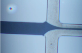
A focused stream at chip scale
The project brought together microchannel fabrication, patterned metal features, and fluid testing. Two side streams squeeze a central sample stream into a narrow path, establishing the fluidic foundation for a chip-scale cytometer.
My work included fabricating the device and testing its flow behavior with three syringes: red dye in the central inlet and water in the two side inlets.

From wafer to sealed channels
The fabrication sequence used photolithography and wet etching to define channels in silicon, thermal oxidation to form an insulating oxide layer, aluminum deposition and patterning for electrodes, and anodic bonding to a Pyrex 7740 cover.
The process included S1813 photoresist, buffered oxide etch, KOH channel etching, approximately 0.5 µm of dry thermal oxide, and approximately 250 nm of aluminum. Fabrication observations included nonuniform oxide color.

Processes and equipment
I worked through the fabrication sequence from patterned resist and etched silicon to metal features and a bonded glass cover. Each stage prepared the wafer for the next operation.
Used S1813 and SJR5740 photoresists to define features for the channel and electrode process steps, with CD26 development.
Opened the oxide mask with BOE and used temperature-controlled KOH etching to form the silicon microchannels.
Grew approximately 0.5 µm of dry thermal oxide to provide an insulating layer on the silicon.
Deposited approximately 250 nm of aluminum by thermal evaporation, then patterned the metal with lithography and PAN wet etching.
Bonded the processed silicon to a drilled Pyrex 7740 cover to enclose the fluidic channels.
Introduced central red dye and side water streams, then observed their behavior at the focusing junction under the microscope.
Demonstrating hydrodynamic focusing
The syringe test produced a thin focused dye stream with no observed leakage or backflow. This demonstrated successful fluidic operation of the fabricated channels and bonded assembly.
Hydrodynamic focusing was observed. Electrical measurements and cell-counting performance were not evaluated in this test.